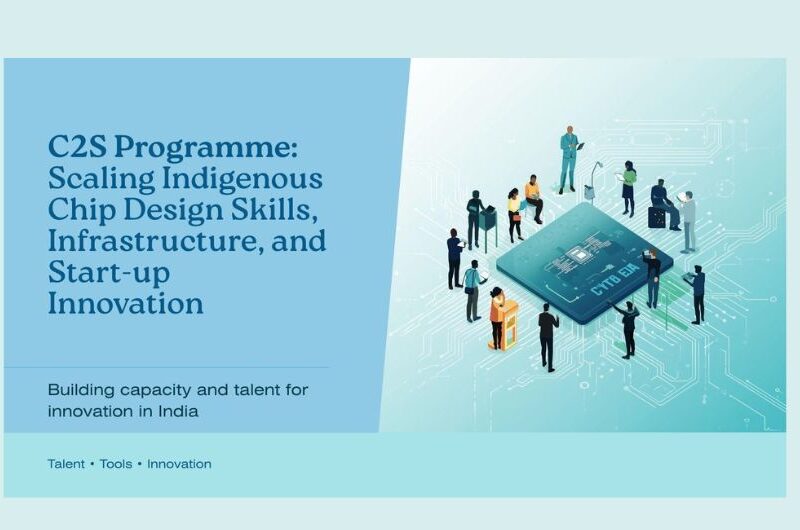
C2S Programme: Scaling Indigenous Chip Design Skills, Infrastructure, and Start-up Innovation 1. Chips to Start-up Programme is a national capacity-building initiative launched in 2022, with ₹250 crore over five years, expanding chip design education, fabrication exposure, and innovation across institutions. 2. It targets creation of 85,000 industry-ready professionals across UG, PG, and PhD levels nationwide, including 200 PhDs, 7,000 VLSI M.Tech, 8,800 allied M.Tech, and 69,000 B.Tech trainees overall. 3. Nearly one lakh individuals enrolled for chip design training, and about 67,000 have been trained so far, addressing global semiconductor talent shortages and strengthening domestic skill pipelines rapidly. 4. Programme ecosystem spans about 400 organisations: 305 academic institutions under C2S and 95 startups under a complementary incentive scheme, widening participation beyond elite campuses nationwide into innovation networks. 5. It aims to catalyse 25 start-ups and enable 10 technology transfers, while expanding SMART lab access, training one lakh students, generating 50 patents, and supporting 2,000 research publications. 6. Hands-on learning is delivered through industry-led training, mentorship, and access to advanced EDA software, foundry interfaces, fabrication facilities, and testing resources for designing, building, and validating chips securely. 7. Participating institutions pursue prototypes of ASICs, Systems-on-Chip, and reusable IP cores, bridging curriculum learning with full workflows from architecture and verification to tape-out, fabrication, testing, and post-silicon evaluation. Coordinating Organization Mode Area 100+ Participating Academic Institutions (Beneficiaries of project funds, EDA Tools & trainings) Implementation of R&D projects for design & fabrication (2–5 years) Instruction as part of curriculum, Short-term courses, labs, and student projects (including nearby institutions). End-to-end exposure to chip design, fabrication, and testing through R&D projects 200+ Other Organizations (Beneficiaries of EDA Tools & trainings) Instruction as part of curriculum, Short-term courses, labs, and student projects. General chip design flows using advanced EDA tools. ChipIN Centre, C-DAC Bangalore (Serving 300+ institutions) Regular training sessions with industry partners. Facilities include: Specialized design areas using advance tools. EDA tools Synopsys, Cadence, IBM, Siemens EDA, Ansys, Keysight Technologies, Silvaco, AMD, Renesas Foundry access SCL, IMEC, MUSE Semiconductors Chip design flow ChipIN Centre, NIELIT SMART Lab, NIELIT Calicut (Pan-India institutions) Identified short-term and certification courses. General chip design flows using centralized hardware resources. 8. ChipIN Centre at C-DAC Bengaluru functions as a national shared design infrastructure hub, supporting 300+ institutions with tools, compute, IP libraries, mentoring, and structured design onboarding services nationwide. 9. ChipIN Centre conducted six shared wafer runs and 265+ training sessions, while addressing 4,855 support requests, demonstrating sustained technical assistance and operational scale for academic chip programmes nationwide. 10. Designs are collected, verified for fabrication readiness, iterated with feedback, aggregated onto shared wafers, and sent every three months to SCL Mohali for fabrication using 180 nm technology. 11. SCL Mohali enabled large-scale hands-on design: 122 submissions from 46 institutions, with 56 student-designed chips successfully fabricated, packaged, tested, and delivered back for real silicon validation for learning. 12. Shared national EDA infrastructure recorded over 175 lakh hours of tool usage by users across 400 organisations, indicating intensive practical engagement with professional-grade electronic design automation platforms nationwide. 13. Institutions filed 75+ patents and are developing 500+ IP cores, ASICs, and SoC designs, with applications spanning defence, telecom, automotive, consumer electronics, and industrial systems integration nationwide today. 14. FPGA boards were distributed through centralised and distributed models to support prototyping and design validation, complemented by high-performance computing access via the PARAM Utkarsh supercomputer resources nationally effectively. 15. Coordinated institutional framework links policy direction, funding, and oversight with infrastructure operators and fabrication facilities, ensuring equitable access, stronger academia–industry collaboration, and a steady pipeline of chip designers. Must-Know Terms : 1.Chips to Start-up (C2S) Programme: Chips to Start-up is a MeitY capacity-building umbrella launched in 2022 to democratise chip design. It funds training, curriculum integration, labs, and R&D projects, linking students with industry mentors and national infrastructure. Its targets include 85,000 professionals, start-up incubation, patents, technology transfers, and silicon validation, strengthening self-reliant design capability across diverse institutions nationwide, including smaller colleges too, for long-term resilience. 2.ChipIN Centre: ChipIN Centre, operated by C-DAC Bengaluru, provides shared semiconductor design infrastructure for hundreds of institutions. It offers commercial EDA tool access, compute, IP libraries, onboarding, and mentoring. It aggregates student designs, verifies fabrication readiness, and organises periodic multi-project wafer submissions. It also runs frequent training and resolves technical support tickets, accelerating hands-on learning and reproducible design outcomes consistently, nationwide regularly. 3.Shared Wafer Run: A shared wafer run pools multiple validated chip layouts from different teams onto one wafer, reducing fabrication costs per participant. ChipIN collects designs, checks rule compliance, coordinates iterations, and tapes out combined masks. SCL fabricates the wafer, then packages and returns individual dies. This approach enables students to experience real fabrication cycles, post-silicon testing, and design improvement loops quickly, repeatedly. 4.Electronic Design Automation (EDA) Tools: EDA tools are professional software suites used to design, simulate, verify, and layout integrated circuits. They support steps like RTL coding, synthesis, timing analysis, place-and-route, signoff checks, and verification. Access to commercial platforms through shared national infrastructure lets learners practice industry workflows, reduce errors before fabrication, and build reusable design blocks that meet foundry requirements reliably, at scale, and compliance. 5.Semi-Conductor Laboratory (SCL) Mohali and 180 nm: SCL Mohali provides fabrication and packaging support for student designs under the programme. Designs are manufactured using an established 180 nanometre process, suitable for training, prototyping, and many control-oriented applications. After fabrication, chips are packaged and delivered back to teams for validation. This closes the loop from design to silicon, making learning evidence-based and measurable for institutions nationwide, and confidence. 6.FPGA and PARAM Utkarsh Support: Field Programmable Gate Arrays let designers prototype digital logic and verify functionality before committing to fabrication, cutting risk and iteration time. The programme supplies FPGA boards through central and distributed modes for labs and projects. High-performance computing via the PARAM Utkarsh supercomputer supports demanding EDA workloads and simulations. Together, they enable scalable learning, faster verification, and more robust tape-outs effectively. Key Takeaways Over 1 lakh individuals have enrolled in chip design training, with approximately 67,000 trained so far.
More Details