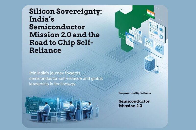
Silicon Sovereignty: India’s Semiconductor Mission 2.0 and the Road to Chip Self-Reliance
1. ISM 2.0 in Budget 2026–27 prioritises domestic semiconductor equipment and materials, full-stack Indian semiconductor IP, and stronger supply chains, backed by ₹1,000 crore for FY 2026–27 allocation nationwide.
2. India’s semiconductor market is estimated at $38 billion in 2023, $45–$50 billion in 2024–25, and projected to reach $100–$110 billion by 2030, driven by demand across value chains.
3. ISM 1.0, approved in December 2021, created an incentive framework of ₹76,000 crore, offering fiscal support up to 50% for silicon fabs, compound semiconductors, ATMP/OSAT, and design nationwide.
4. By December 2025, ten semiconductor projects totaling ₹1.60 lakh crore were approved across six states, spanning silicon fabs, silicon carbide fabs, advanced packaging, memory packaging, and testing infrastructure.
5. By 2029, India targets capability to design and manufacture chips covering 70–75% of domestic applications, serving consumer appliances, industrial electronics, automobiles, telecommunications, aerospace, and power electronics sectors needs.
6. The advanced manufacturing roadmap defines progression toward 3-nanometre and 2-nanometre nodes, aiming for India to rank among top semiconductor nations by 2035 through sustained capability building and resilience.
7. For 2026–27, the modified semiconductor and display manufacturing ecosystem programme carries a total outlay of ₹8,000 crore, recalibrating support for manufacturing, display fabs, and the design ecosystem nationwide.
8. In 2026–27, the modified scheme for semiconductor fabs supports one fab, targeting ₹4,000 crore investment during the year and generating about 1,500 jobs in operations and engineering directly.
9. The compound semiconductors, photonics, sensors, discrete fabs and ATMP/OSAT scheme supports nine units in 2026–27, targeting ₹11,000 crore investment and about 3,000 jobs across facilities for capacity scaling.
10. The design-linked incentive scheme supports 30 design companies in 2026–27, targeting development of 10 semiconductor IP cores and employment of around 200 specialised semiconductor design professionals this year.
11. By January 2026, design incentives support 24 startups, which attracted nearly ₹430 crore venture funding, while the national EDA platform recorded about 2.25 crore high-end tool hours nationally.
12. Around 67,000 students and over 1,000 startup engineers use national design tools; academia completed 122 tape-outs and fabricated 56 chips at 180 nm in the Mohali facility annually.
13. Startups completed 16 tape-outs, producing six chips at advanced foundry nodes including 12 nm; academic institutions filed 75 patents and startups filed 10 patents, expanding indigenous IP rapidly.
14. DHRUV64 is an indigenous 64-bit microprocessor built by C-DAC under MDP, intended for 5G, automotive electronics, industrial automation, consumer devices, and IoT, reducing import dependence and security assurance.
15. Talent pipeline measures include Chips to Startup across 397 universities and startups, AICTE semiconductor programmes, SMART Lab training over 62,000 engineers toward 100,000, and Lam partnership training 60,000.
Must Know Terms :
1.India Semiconductor Mission 2.0 (ISM 2.0):
ISM 2.0 is the Budget 2026–27 push to move from ecosystem creation to consolidation. It prioritises domestic semiconductor equipment and materials, full-stack Indian IP, and stronger supply chains. The government earmarked ₹1,000 crore for FY 2026–27 to support industry-led R&D and training centres, aiming to deepen technology capability and workforce readiness across the entire chip value chain.
2.Modified Semiconductor & Display Programme (2026–27):
This is the recalibrated support package responding to global incentive competition. For 2026–27, it carries a total financial outlay of ₹8,000 crore to accelerate capital investment across semiconductor fabs, compound semiconductors, ATMP/OSAT, and display manufacturing. It focuses on expanding fabrication, packaging, and design capacity, generating high-quality jobs, and reducing dependence on concentrated global suppliers and shocks.
3.Design Linked Incentive (DLI) Scheme:
DLI strengthens India’s fabless and IP creation pipeline by supporting startups and early-stage design firms. As of January 2026, it supports 24 design startups, which attracted nearly ₹430 crore venture funding. It aims to translate academic research into deployable products, increase patents and tape-outs, and scale toward enabling at least 50 fabless companies in the next phase.
4.Advanced EDA National Chip Design Platform:
Advanced Electronic Design Automation access is the backbone for domestic chip design at scale. The platform has recorded around 2.25 crore tool hours, with about 67,000 students and over 1,000 startup engineers using high-end tools. It lowers entry barriers, improves design productivity, and supports more tape-outs and prototypes by providing shared infrastructure that individual institutions may not afford independently.
5.Tape-out and Fabrication Pipeline (Mohali SCL + Advanced Nodes):
Tape-out is the stage where a design is finalised for fabrication, making it a measurable output of design capability. Academia has completed 122 tape-outs, with 56 chips fabricated at 180 nm at the Semiconductor Laboratory, Mohali. Startups completed 16 tape-outs, producing six chips at advanced foundry nodes including 12 nm, signalling progress beyond legacy processes.
6.DHRUV64 and Indigenous Microprocessor Stack:
DHRUV64 is an indigenous 64-bit microprocessor developed by C-DAC under the Microprocessor Development Programme. It is positioned for deployment in 5G infrastructure, automotive electronics, industrial automation, consumer devices, and IoT. It builds on SHAKTI, AJIT, VIKRAM, and THEJAS under the DIR-V programme using RISC-V architecture, improving sovereignty and security in critical computing.
Key Takeaways
- Union Budget 2026–27 allocates ₹1,000 crore for India Semiconductor Mission (ISM) 2.0.
- As of December 2025, 10 ISM projects worth ₹1.60 lakh crore approved across six states.
- India’s semiconductor market projected to reach $100–110 billion by 2030.
MCQ :
1. India Semiconductor Mission 2.0 announced in Budget 2026–27 primarily emphasises which strategic shift?
A) Import substitution through tariff protection
B) Consolidation of domestic capabilities across equipment, materials, IP, and supply chains
C) Exclusive focus on consumer electronics manufacturing
D) Privatisation of semiconductor regulation
2. The financial provision made specifically for ISM 2.0 in FY 2026–27 is:
A) ₹500 crore
B) ₹750 crore
C) ₹1,000 crore
D) ₹1,500 crore
3. India’s semiconductor market size is projected to reach approximately what value by 2030?
A) $60–70 billion
B) $80–90 billion
C) $100–110 billion
D) $130–140 billion
4. The incentive framework approved under India Semiconductor Mission 1.0 amounted to:
A) ₹45,000 crore
B) ₹60,000 crore
C) ₹76,000 crore
D) ₹1,00,000 crore
5. By December 2025, how many semiconductor projects had been approved under ISM across Indian states?
A) Six
B) Eight
C) Ten
D) Twelve
6. By 2029, India aims to meet what proportion of its domestic chip application requirements through indigenous capability?
A) 40–45 per cent
B) 55–60 per cent
C) 70–75 per cent
D) 85–90 per cent
7. The advanced manufacturing roadmap under ISM envisions achieving which technology nodes in the long term?
A) 10 nm and 7 nm
B) 7 nm and 5 nm
C) 5 nm and 3 nm
D) 3 nm and 2 nm
8. The total financial outlay for the modified semiconductor and display manufacturing programme in 2026–27 is:
A) ₹6,000 crore
B) ₹7,000 crore
C) ₹8,000 crore
D) ₹9,000 crore
9. Under the modified semiconductor fab scheme for 2026–27, how many fabs are proposed to be supported?
A) One
B) Two
C) Three
D) Four
10. The compound semiconductor, photonics, sensors, and ATMP/OSAT scheme in 2026–27 supports how many units?
A) Five
B) Seven
C) Nine
D) Eleven
11. The Design Linked Incentive Scheme in 2026–27 targets support for how many design companies?
A) 20
B) 25
C) 30
D) 40
12. As of January 2026, semiconductor design startups supported under DLI attracted venture funding of nearly:
A) ₹250 crore
B) ₹320 crore
C) ₹430 crore
D) ₹600 crore
13. Approximately how many high-end EDA tool hours have been recorded on the national chip design platform?
A) 1.25 crore
B) 1.75 crore
C) 2.25 crore
D) 3.00 crore
14. DHRUV64, India’s indigenous 64-bit microprocessor, has been developed by:
A) ISRO
B) DRDO
C) C-DAC
D) BEL
15. DHRUV64 and related indigenous processors are based on which open architecture?
A) ARM
B) x86
C) MIPS
D) RISC-V

0 comment