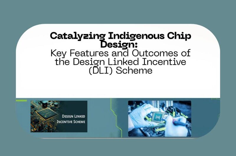
Catalyzing Indigenous Chip Design: Key Features and Outcomes of the Design Linked Incentive (DLI) Scheme
Key Takeaways
- Semiconductor chip design is the main value driver, contributing up to 50% of value addition, 20–50% of Bill of Materials cost (BOM), and 30–35% of global semiconductor sales via the fabless segment.
- MeitY’s Design Linked Incentive (DLI) Scheme under the Semicon India Programme aims to build a self-reliant, globally competitive chip design ecosystem.
- 24 DLI-supported chip design projects target strategic sectors including video surveillance, drone detection, energy metering, microprocessors, satellite communications, and IoT SoCs.
- DLI supported projects are scaling rapidly, with 16 tape-outs, 6 ASICs chips, 10 patents, 1,000+ engineers engaged, and over 3× private investment leveraged.
1. Chip design drives semiconductor value, contributing up to half value addition, 20–50% bill of materials cost, and 30–35% global sales in fabless segment overall.
2. Design Linked Incentive scheme aims to build a self-reliant, globally competitive fabless ecosystem by supporting domestic startups, MSMEs, and indigenous intellectual property creation domestically.
3. Twenty-four supported chip design projects target strategic domains: video surveillance, drone detection, energy metering, microprocessors, satellite communications, and broadband or IoT systems-on-chip security applications.
4. Supported projects show rapid scaling: sixteen tape-outs completed, six ASIC chips fabricated, ten patents filed, over one thousand engineers engaged, leveraging triple private investment.
5. Fabless companies capture high strategic value because design and IP determine product intelligence, efficiency, and security, while requiring modest capital expenditure relative to fabrication.
6. Eligibility covers startups and MSMEs for incentives plus design infrastructure, while other domestic companies can receive financial incentives for deploying semiconductor designs successfully nationwide.
7. Product design support reimburses up to fifty percent eligible expenditure, capped at fifteen crore rupees per application, covering ICs, chipsets, SoCs, systems, IP cores.
8. Deployment incentive provides six to four percent of net sales turnover for five years, capped at thirty crore rupees, subject to cumulative sales thresholds.
9. ChipIN Centre provides shared infrastructure: remote national EDA tool grid, IP core repository access, MPW prototyping fiscal support, and post-silicon validation assistance for startups.
10. ChipIN democratized advanced EDA access for about one lakh engineers and students across four hundred organizations, including academic institutions and many supported startups nationwide.
11. National shared EDA Grid recorded 54,03,005 cumulative usage hours by ninety-five supported startups as of 2 January 2026, indicating strong nationwide tool adoption rates.
12. Outcomes include ten patents, sixteen tape-outs, six silicon-proven chips, over one thousand specialized engineers trained or engaged, and more than 140 reusable IP cores.
13. Semicon India Programme, with seventy-six thousand crore rupees outlay, supports semiconductor and display manufacturing and design ecosystem, with implementation support from C-DAC as agency.
14. Chips to Startup programme builds capacity across institutions to generate eighty-five thousand industry-ready chip-design professionals, while microprocessor efforts produced VEGA, SHAKTI, AJIT families domestically.
15. Success cases include motor-control BLDC chips, indigenous RISC-V processor IPs, AI-capable surveillance SoCs in 12 nm, broadband GPON solutions, and radar-on-chip development pipelines globally.
MCQ:
1. Semiconductor chip design contributes up to which share of value addition in the semiconductor value chain?
A. 10%
B. 25%
C. 50%
D. 75%
2. Design and IP typically account for what share of a semiconductor’s value, as highlighted in the explainer?
A. Less than 10%
B. About one-third
C. More than half
D. Nearly all of it
3. Under the scheme, reimbursement for product design support is capped at:
A. ₹10 crore per application
B. ₹15 crore per application
C. ₹20 crore per application
D. ₹30 crore per application
4. Deployment-linked incentive under the scheme is provided as:
A. 10%–8% of gross sales for 3 years
B. 6%–4% of net sales turnover for 5 years
C. 4%–2% of net sales turnover for 10 years
D. Fixed grant of ₹30 crore for 5 years
5. The deployment-linked incentive cap per application is:
A. ₹15 crore
B. ₹25 crore
C. ₹30 crore
D. ₹76,000 crore
6. Minimum cumulative net sales required over Years 1–5 for startups/MSMEs is:
A. ₹50 lakh
B. ₹1 crore
C. ₹2 crore
D. ₹5 crore
7. Minimum cumulative net sales required over Years 1–5 for other domestic companies is:
A. ₹1 crore
B. ₹2 crore
C. ₹5 crore
D. ₹10 crore
8. The design must be successfully deployed in electronic products for obtaining:
A. Product design reimbursement
B. Access to EDA tools
C. Deployment-linked incentive
D. MPW prototyping fiscal support
9. Which set correctly lists the main design infrastructure supports offered through the ChipIN Centre?
A. EDA grid, IP core repository, MPW prototyping, post-silicon validation
B. Waiver of customs duties, land subsidy, power tariff discount, export rebate
C. Patent filing waiver, GST exemption, freight subsidy, credit guarantee
D. Salary support, rent subsidy, marketing grant, equity infusion
10. The scheme was launched in:
A. December 2019
B. December 2020
C. December 2021
D. December 2022
11. About 1 lakh engineers and students across 400 organizations gained access to advanced EDA tools primarily through:
A. A private EDA marketplace
B. A centralized facility user base via ChipIN
C. Bilateral technology transfer treaties
D. A semiconductor import substitution tariff
12. As of 2 January 2026, cumulative usage recorded on the shared EDA Grid was:
A. 5,40,305 hours
B. 54,03,005 hours
C. 5,43,00,500 hours
D. 4,05,300 hours
13. Which of the following outcomes is correctly matched with the supported ecosystem performance?
A. 16 patents filed, 10 tape-outs completed, 6 chips designed
B. 10 patents filed, 16 tape-outs completed, 6 chips fabricated
C. 6 patents filed, 16 chips fabricated, 10 tape-outs completed
D. 10 tape-outs filed, 6 patents completed, 16 chips fabricated
14. The total outlay mentioned for the broader programme supporting manufacturing and design is:
A. ₹7,600 crore
B. ₹16,000 crore
C. ₹76,000 crore
D. ₹1,76,000 crore
15. Chips to Startup capacity-building target is to generate approximately:
A. 8,500 industry-ready professionals
B. 35,000 industry-ready professionals
C. 85,000 industry-ready professionals
D. 1,85,000 industry-ready professionals

0 comment